


Engineers develop a hybrid process that connects photonics with “artificial atoms,” to produce the largest quantum chip of its type.
MIT researchers have developed a process to manufacture and integrate “artificial atoms,” created by atomic-scale defects in microscopically thin slices of diamond, with photonic circuitry, producing the largest quantum chip of its type.
The accomplishment “marks a turning point” in the field of scalable quantum processors, says Dirk Englund, an associate professor in MIT’s Department of Electrical Engineering and Computer Science. Millions of quantum processors will be needed to build quantum computers, and the new research demonstrates a viable way to scale up processor production, he and his colleagues note.
Unlike classical computers, which process and store information using bits represented by either 0s and 1s, quantum computers operate using quantum bits, or qubits, which can represent 0, 1, or both at the same time. This strange property allows quantum computers to simultaneously perform multiple calculations, solving problems that would be intractable for classical computers.
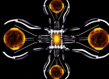
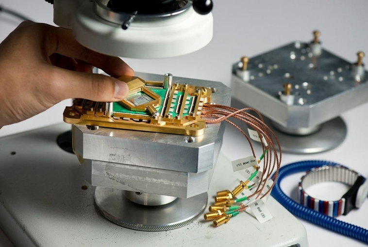
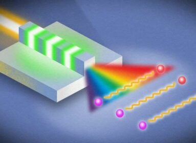
The qubits in the new chip are artificial atoms made from defects in diamond, which can be prodded with visible light and microwaves to emit photons that carry quantum information. The process is a hybrid approach, in which carefully selected “quantum micro chiplets” containing multiple diamond-based qubits are placed on an aluminum nitride photonic integrated circuit.
“In the past 20 years of quantum engineering, it has been the ultimate vision to manufacture such artificial qubit systems at volumes comparable to integrated electronics,” Englund says. “Although there has been remarkable progress in this very active area of research, fabrication and materials complications have thus far yielded just two to three emitters per photonic system.”
Using their hybrid method, Englund and colleagues were able to build a 128-qubit system — the largest integrated artificial atom-photonics chip yet.“
The artificial atoms in the chiplets consist of color centers in diamonds, defects in diamond’s carbon lattice where adjacent carbon atoms are missing, with their spaces either filled by a different element or left vacant. In the MIT chiplets, the replacement elements are germanium and silicon. Each center functions as an atom-like emitter whose spin states can form a qubit. The artificial atoms emit colored particles of light, or photons, that carry the quantum information represented by the qubit.
Diamond color centers make good solid-state qubits, but “the bottleneck with this platform is actually building a system and device architecture that can scale to thousands and millions of qubits,” Wan explains. “Artificial atoms are in a solid crystal, and unwanted contamination can affect important quantum properties such as coherence times. Furthermore, variations within the crystal can cause the qubits to be different from one another, and that makes it difficult to scale these systems.”
Instead of trying to build a large quantum chip entirely in diamond, the researchers decided to take a modular and hybrid approach. “We use semiconductor fabrication techniques to make these small chiplets of diamond, from which we select only the highest quality qubit modules,” says Wan. “Then we integrate those chiplets piece-by-piece into another chip that ‘wires’ the chiplets together into a larger device.”
“The diamond color centers emit in the visible spectrum. Traditional silicon, however, absorbs visible light, which is why we turn to aluminum nitride for our photonics platform, as it is transparent in that regime,” Lu explains. “Furthermore, aluminum nitride can support photonic switches that are functional at cryogenic temperatures, which we operate at for controlling our color centers.”
Using this hybrid approach of photonic circuits and diamond chiplets, the researchers were able to connect 128 qubits on one platform. The qubits are stable and long-lived, and their emissions can be tuned within the circuit to produce spectrally indistinguishable photons, according to Wan and colleagues.

While the platform offers a scalable process to produce artificial atom-photonics chips, the next step will be to “turn it on,” so to speak, to test its processing skills.
“This is a proof of concept that solid-state qubit emitters are very scalable quantum technologies,” says Wan. “In order to process quantum information, the next step would be to control these large numbers of qubits and also induce interactions between them.”
The qubits in this type of chip design would not necessarily have to be these particular diamond color centers. Other chip designers might choose other types of diamond color centers, atomic defects in other semiconductor crystals like silicon carbide, certain semiconductor quantum dots, or rare-earth ions in crystals.
“Because the integration technique is hybrid and modular, we can choose the best material suitable for each component, rather than relying on natural properties of only one material, thus allowing us to combine the best properties of each disparate material into one system,” says Lu.
Finding a way to automate the process and demonstrate further integration with optoelectronic components such as modulators and detectors will be necessary to build even bigger chips necessary for modular quantum computers and multichannel quantum repeaters that transport qubits over long distances, the researchers say.
Source: Becky Ham | MIT News correspondent


Comments are closed.